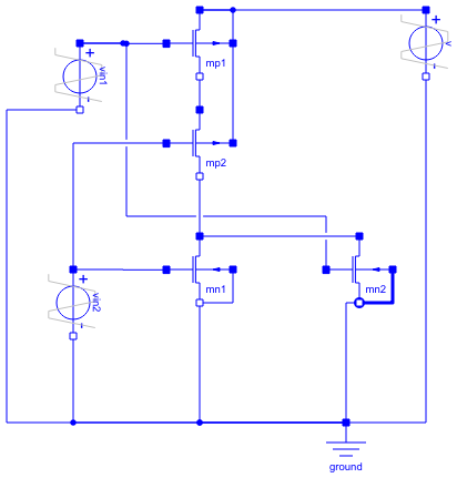
NorMOS NOR gate circuit |
|
Diagram
Information
This information is part of the Modelica Standard Library maintained by the Modelica Association.
In nearly every electronic the basic circuit "nor" is used. A nor contains two PMOS and two NMOS. The faulty wiring can be seen in the graphical mode. If and only if the two input voltages have low potential, the output voltage has high potential, otherwise the output voltage has low potential.
Nor truth table (1 means true, it is represented by the 5V voltage):
input voltage vin1 |
input voltage vin2 |
output voltage mp1.S |
0 |
0 |
1 |
0 |
1 |
0 |
1 |
0 |
0 |
1 |
1 |
0 |
Simulate until t=5s. Display the two input voltages vin1.p.v and vin2.p.v and the output voltage mp1.S.v.
The output value in the example shows a behaviour "near" the one of the truth table, since the capacitances are huge. Therefore loading is not finished before the next input changes.