DifferenceAmplifierSimple NPN transistor amplifier circuit |
|
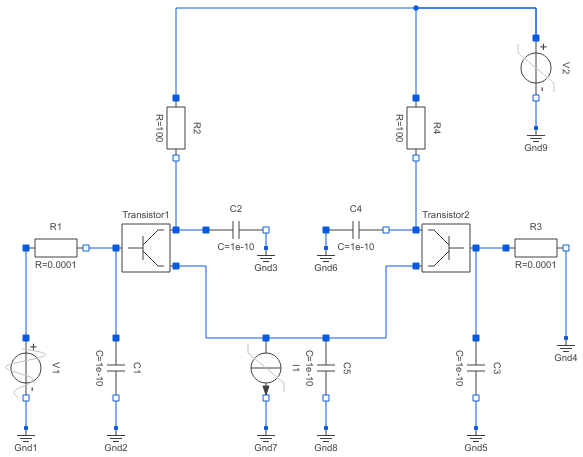
Diagram
Information
This information is part of the Modelica Standard Library maintained by the Modelica Association.
It is a simple NPN transistor amplifier circuit. The voltage difference between R1.p and R3.n is amplified. The output signal is the voltage between R2.n and R4.n. In this example the voltage at V1 is amplified because R3.n is grounded.
The simulation end time should be set to 1e- 8. Please plot the input voltage V1.v, and the output voltages R2.n.v, and R4.n.v.
Reference:
Tietze, U.; Schenk, Ch.: Halbleiter-Schaltungstechnik. Springer-Verlag Berlin Heidelberg NewYork 1980, p. 59
Components (23)
| V1 |
Type: ExpSineVoltage |
|
|---|---|---|
| V2 |
Type: RampVoltage |
|
| I1 |
Type: RampCurrent |
|
| R1 |
Type: Resistor |
|
| R2 |
Type: Resistor |
|
| R3 |
Type: Resistor |
|
| R4 |
Type: Resistor |
|
| C1 |
Type: Capacitor |
|
| C4 |
Type: Capacitor |
|
| C5 |
Type: Capacitor |
|
| C2 |
Type: Capacitor |
|
| C3 |
Type: Capacitor |
|
| Gnd1 |
Type: Ground |
|
| Gnd9 |
Type: Ground |
|
| Gnd3 |
Type: Ground |
|
| Gnd2 |
Type: Ground |
|
| Gnd6 |
Type: Ground |
|
| Gnd7 |
Type: Ground |
|
| Gnd8 |
Type: Ground |
|
| Gnd5 |
Type: Ground |
|
| Gnd4 |
Type: Ground |
|
| Transistor1 |
Type: Transistor |
|
| Transistor2 |
Type: Transistor |